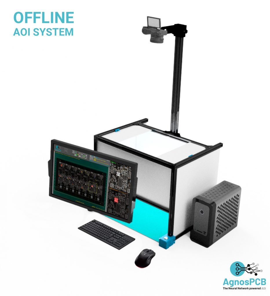
Elements:
- SONY Alpha camera
- 50mm F1.8 Autofocus LENS
- 2x 30W Led Lighting panels (dimmable)
- Light diffusers
- Black anodized aluminum structure
- Height adjustable camera mast
- ESD Mat (Anti-static mat) + Ground lead
- Battery dummy + 2m USB cable
- Processing unit: in charge of locally processing all the data captured.
You will get the inspection platform KIT, pre-assembled.
Interactive 3D model
How to set everything up: assembly process
The inspection platform KIT has been preassembled. Basically, you just need to insert the camera’s mast into its vertical channel and connect the camera.
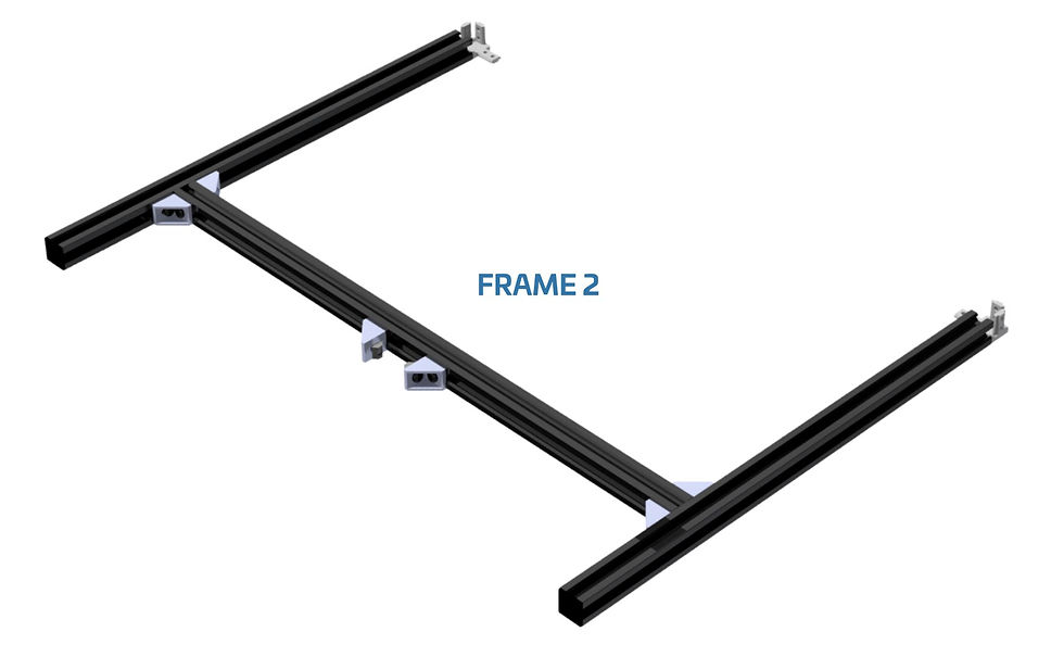
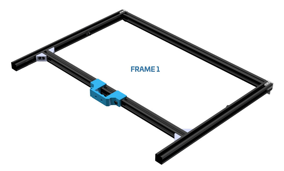
You will find, after opening the box containing the KIT´s parts, two square frames as the ones shown below.
FRAME 2 is the base of the inspection platform. FRAME 1, the upper element of the structure. As indicated, everything has been pre-assembled as these images:
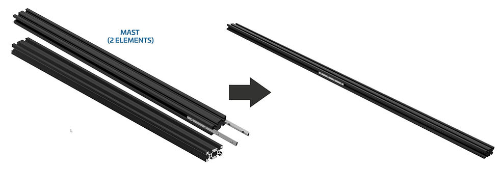
STEP 1:
Insert one of the 2040 aluminum rails inside the other in order to create the MAST. The two lateral rail connectors will make it solid as a unique part. Tighten up the 4 bolts you they have.
STEP 2:
Insert both of the 40cm long 2020 aluminum rails as shown below. Push them to the very end and tighten the headless bolts while pushing.

STEP 3:
Now, insert the MAST between the two triangular metal angle supports but keeping both nuts oriented, so you can slide, easily, the mast into its place. Do not completely tight the two side bolts, you need to leave them loose for now.

Do not completely tight the two side bolts, you need to leave them loose for now.

STEP 4:
Place the 3 white diffusers as indicated below. They will let you know what is the right height of the FRAME 2. With the KIT you got 3 light diffuser: 1x 50×30 cms (to be placed at the back of the inspection area) + 2x 40x30cms (they will be the laterals of the “inspection container”

STEP 5:
Insert the FRAME 1 sliding it using the mast as guide. The diffusers and frontal aluminum rails, will let you know the correct level of this FRAME 1. Once set, tighten the bolts you will find in the back plastic part and the base bolts you left loose in the STEP 3. Detailed image below.


STEP 6:

The lateral LED panels have to be attached to the upper rails using the bolts already located in the blue plastic parts. Use the silver bolts to attach the LED panels to the plastic parts. You can pass the power cables through the gap you can find between the back and lateral diffuser panels.

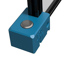
If you got the micro-computer with your inspection platform KIT, you have to fix the trigger button provided to the base of the right aluminum rail using a bolt and NUT as the image. Do not fully tighten the bolt yet:

STEP 7:
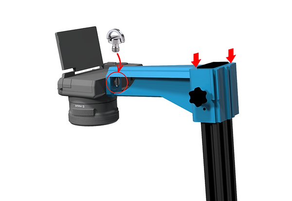
Attach the camera to the ARM palstic part using a camera screw. Then, insert the ARM into the MAST and fix it using the lateral bolt. Done. The last step would be placing the ESD mat under the structure and connect the ground lead to any GROUND connection you have near the inspection platform.

The SONY camera will use a battery DUMMY, so it can be ON for unlimited time. That battery dummy needs a 5V and 3A power supply (provided with the KIT). At the same time, the camera will be controlled from the computer, so use the provided High-speed 2m USB-micro USB cable to connect the camera to any available USB port of the laptop.
SONY CAMERA. Notes.
You got the SONY camera with the 50 mm 1.8f fixed lens already pre-configured but, if accidentally, its photo settings change you will need to set them again as below:
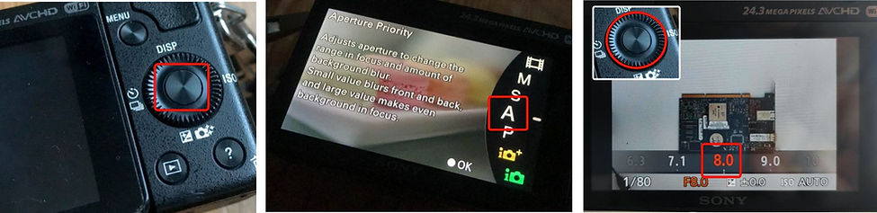
1) Set the mode dial to A (Aperture Priority) pressing the round button and selecting the A mode.
2) Select the value F7.1 by turning the control dial (right image). Setting the aperture to 7.1 will let you get the most detailed photos of your PBCAs
3) Pressing the MENU button, go to setting and set the AEL w/shutter to ON
4) inside the same MENU, the last tab has an option called USB connection. Set it to PC REMOTE.


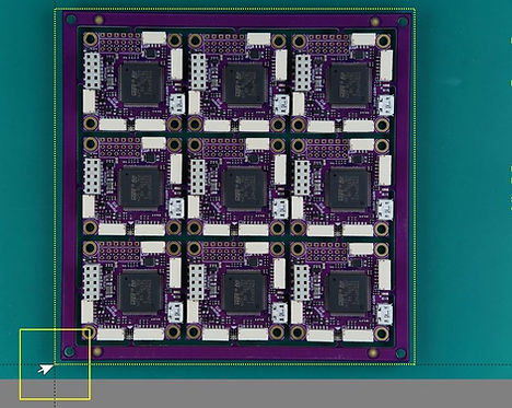
IMPORTANT: all the PCB to be inspected have to be perfectly leveled. If the panel/circuit has a certain tilt angle, not all the elements shapes will be perfectly defined limiting the software recognition capacities.
To capture the whole dimension of the panel / circuit you are inspected, move the camera UP in the mast. For smaller circuits/ panel, move it down but never use digital zoom.
Do not use the DIGITAL ZOOM with the 50mm optics system. It will only artificially increase the size of the digital image not adding real info to the photograph.
If you change any parameter or adjust the camera while the system is ON, the camera will get unresponsive. You will need to disconnect it from the laptop and reconnect it again.

If everything is fine, you will get highly detailed photographs of your PCBa. Above, example of two photos taken with the inspection platform. No shadows cast nor direct light reflections are present.
Connecting the platform to the Agnospcb laptop
With this configuration, the laptop will be in charge of taking the photos using the best possible camera parameters. The computer will do everything for you. Just pushing the ACTION button, you execute almost all the steps of the inspection process.
First, you need to connect everything as indicated below:
1) Connect the 2m USB cable from the CAMERA micro-usb port to a laptop´s USB port.
2) Insert the battery DUMMY into the CAMERA´s battery slot, and connect it to the provided 5V/3A USB power supply. See the diagrams below for details.
3) Connect the second 2m USB cable from INSPECTION BUTTON to another laptop´s USB port.
4) Plug both LED panels into 110 or 220V sockets. Both LED panels light emission can be adjusted and turned ON/OFF using a single remote control (provided). Note that both lights have a master power switch.
It does not matter to which USB port you connect the CAMERA and INSPECTION button, the computer will automatically recognize both devices properly.


How to use the AgnosPCB AOI OFFLINE sytem
Once everything has been connected, the laptop will recognize the camera and inspection button after powering it up.
During the boot sequence, the system will check its own integrity: do no type anything in the unput box displayed. Only AgnosPCB´s technician may ask you to do so.

Below, the video will show you how to “quick-start” using the OFFLINE platform. It provides a glimpse of how this AOI system works. You will find more info about how to get the most of it if you keep reading this guide.

User Interface
Upon launching the Agnospcb inspection tool software, the user interface will appear. It has different panels and inspection areas:
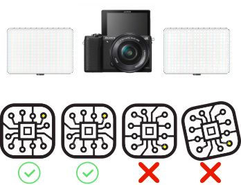
- Reference panel (green ) : The “golden sample” image. Can be loaded using the LOAD icon (from the Reference area).
- Unit Under Inspection (orange): this is the image of the panel to be inspected. Can be loaded using the LOAD icon (from the inspection area)
- Magnification canvas : this frame will display, the same areas of the REFERENCE and RESULT circuit/panels. Move the mouse to check different zones of the circuit. Use the mouse’s wheel to modify the zoom magnification.
- Activity log: provides useful information about the inspection process
- Settings: where the configuration ICONs are. Useful tools in your inspection process.


Start the inspection process. This button is enabled only after you have a REFERENCE and TO BE INSPECTED images already set. Keyboard shortcut: ENTER. When clicked, the AOI will inspect the image taken for the circuit/panel and look for faults. If the Auto-analysis is enabled, the AOI will automatically inspect the last photo taken, so this button will be disabled.

LOAD photo: Use this ICON to load a “reference” or “to be inspected” photo. If you have stored a “reference” image and want to retrieve it to use it again, use this button. You can do the same with an image of a “to be inspected” circuit/ panel. This button will get non-functional if you have the AUTO-PROCESSING option enable, which will automatically process every photo taken with the camera. All the REFERENCE photos can be found inside the folder HOME/APP/REFERENCE. In a folder named after the YEAR-MONTH-DAY-TIME moment when the photo was taken. You can rename the photos as you please.

CROP IMAGE: Useful when the panel/circuit in the photo is too small. Cropping the image will “force” the software to focus in the selected area. Only available in the REFERENCE canvas. The software will automatically look for the same area in every photo taken of the panels to be inspected after it has been set. To remove the CROP boundaries, click on the icon again.

Auto-signalling: In order to highlight the faults detected you have two options: 1) change the color of the faults mask using the Action button “MASK-COLOR” or 2) enabling this feature. It will place a yellow cross on top of the faults detected. Not visible in the magnification areas.

Auto Analyze: if activated, the next photo taken will be automatically processed. That means that the image will be analyzed for faults right after being taken. This option reduces the processing time for every inspection.

Faults Mask-colors: Once the analysis of the panel/circuit has been carried out, the results will be shown as a new mask on top of the image. If faults have been detected, they will be highlighted in red/blue or green. Depending on the PCBA´s color / material you are working with, you may need to change the opacity and color of the mask in order to easily see where those faults are. Every time you click on the ICON the mask color will change. Its opacity can be modified spinning the mouse’s wheel when it is placed on top of the ICON.
The INSPECTION button
The Inspection button will let you take the best possible photo of your circuits / panels just pressing it. It will quickly start the process of configuring the camera with the best parameters, prepare the software, so it can use the latest photo taken, and analyze it looking for faults. Just in a matter of a fraction of a second.
this button can be used for:
1) SET a REFERENCE image: PRESS it for 5 seconds until you hear the camera shooting. The AOI software will use that image as REFERENCE to compare all the next images of the circuits.
2) INITIALIZE the inspection process: Just press it for a second and the camera will capture an image of the circuit / panel to be analyzed. Alternatively, you can click, with the mouse, on the INSPECTION BUTTON (icon below) on the user interface to do the same.

NOTE: if the AUTO ANALYZE button (icon below) has been previously activated, every time you press the INSPECTION button for a second, the image will be inspected automatically. This will help you to reduce the inspection total processing time.

Inspection process
At this point, you should have already set up the inspection platform and everything should be connected to the laptop.
The points listed below will guide you through the steps you need to make to inspect a circuit/ panel your first time. This video shows the same process:
- Turn ON the LEDs panels using the switch and/or remote control. Set, using the UP and DOWN arrows, their brightness. If you are inside a well-lit room, you may not need to set them to their maximum brightness.
- Turn ON the CAMERA.
- Quick-check if the camera is set in aperture mode (A).
- Turn ON the computer and wait for the system to boot.
- The Inspection software tool needs to be launched.
- Check if the camera respond to the INSPECTION BUTTON, pressing it for 5 seconds (or key “R”). That should set a REFERENCE image. This is a photo taken to a circuit/panel you already know is in good condition. As the camera parameters are controlled from the laptop, you do not have to do anything. Just check if the image is in focus. You can use the mouse’s wheel to increase the zoom magnification and take a closer look at the elements.
- Once the REFERENCE photo of the circuit/panel has been set, you can now take photos of the units you want to inspect (units under inspection). Press the INSPECTION BUTTON for one second to take a photo (or key “S”)
- You are ready to go. The system should be now indicating, if any, faults on the UUI (Unit Under Inspection). Go to point 7 and repeat the process once a new UUI has been placed under the camera.
All the inspection results will be stored in the PCB_OUT folder you will find in the external USB drive. The REFERENCE images will be moved to the folder called “REFERENCE”. You can find all of them there , in the case you need any of the REFERENCE images previously used.
NOTE: the “R” key from the keyboard will work as a camera trigger button too. “R” will set a REFERENCE image. “S” will take a photo of an image to be inspected.
NOTE: If you activate the AUTO-ANALYSIS option, all the photos taken pressing “R” or the INSPECTION BUTTON for one second, will be automatically processed.
IMPORTANT: By default, we send the camera already configured, but from time to time, re-check the camera is operating with the Aperture MODE enabled.
First, tap on the round button indicated above. The select rotating the dial, the Aperture MODE (A). Then, using the same dial, select the value F8.0 (right image). Setting the aperture to F8.0 will let you get the most detailed photos of your circuits / panels.
How to get the most of the AOI system
With some tips about how to improve the fault detection results and comments about what not to do.
Light sources and panel/circuit orientation
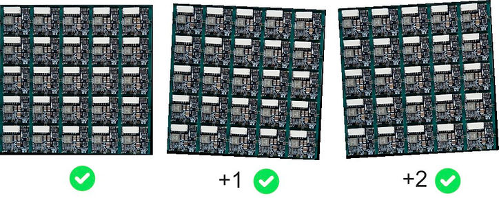
The inspection platform uses 2 LED lights and diffuser panels to get rid of cast shadows. But if you take photos of the circuits varying its orientation every inspection, large electronic elements (like capacitors, coils and connectors) present on the circuits/ panels will be seen differently from the camera’s point of view.
Try to place the circuit always with the same orientation.
The software is capable, within a second, of auto-aligning the images, but the light projected will fall very differently over the electronic components if the circuit is rotated by 90/180 degrees. That will lead the neural network to make mistakes when looking for faults. Try to avoid it always placing the panels/circuits with the same orientation.

Optical / Digital ZOOM
When using a DIGITAL ZOOM, the camera’s optics are not adjusted. It is accomplished electronically, so no optical resolution is gained. That means that you are not providing useful info to the software.
If you are using our inspection platform and are inspecting a small circuit/panel: Move the camera DOWN until it is about 45 cm over from the circuit you are inspecting. The structure of the platform will not allow going down further in any case. From that distance, take the photos.
Do not use the camera controls to increase the size of the circuit/ panel. That will only degrade the quality of the image taken. The laptop will take control of the camera and set the best configuration under every circumstance.
CROPPING tool
Useful when the panel/circuit in the photo is too small. Cropping the image will “force” the software to focus on the selected area and will reduce the inspection time.
You can only crop an image in the REFERENCE canvas.
The software will automatically look for the same area in every photo taken of the panels to be inspected after the cropping boundary has been set. To remove the CROP boundaries, click on the CROP icon again.
In case of doubt, visit the Inspection tool guide.
CIRCUIT / PANEL with many small electronic elements
The neural network powering the Agnospcb software behaves as a very skilled technician. But it can only detect faults that can be seen. Any minor displacement, solder paste change or short-circuit “hidden” under a shadow or light reflection may become identifiable if we slightly change the lighting conditions / orientation of the panel/ circuit.
If you are inspecting a panel/ circuit with electronic elements casting pronounced shadows over other component/s, elements with very small pins or just obstructing the camera point of view, we recommend following this methodology which can lead to increase the detection rate:
1) Run a regular inspection and check results.
2) Slightly rotate the panel/ circuit and run a second inspection.
3) Every inspection takes between 1-4 seconds so, a third one could be done quickly. Run a third inspection but, in this case, rotating in the opposite direction the panel/ circuit.
The vast majority of inspections do not require this methodology, but it is interesting to note the possibility of increasing the detection capability of the system by carrying out this process.
The camera does not respond
Check if the battery dummy is connected to the correct USB power supply, capable of delivering 3A. Check if the USB cable is properly connected and fully inserted. Does the R and S keys of the keyboard trigger the camera?
Need help?
Contact us at:
+1 (619) 503-1003871
info@agnospcb.com